That microchips are ubiquitous has been brought home to us in recent months with their scarcity. Many industries have had to interrupt or reduce production because they were unable to procure the required number of microchips. But how is such a chip designed in the first place? How do you get the complexity of several billion switching elements under control and how do these circuits finally get onto / into the silicon?
The era of semiconductors began with the invention of the transistor in 1947, although it took almost 10 years before the technology was ready for the market or the true value of this component was recognized. In the 1960s, the first integrated circuits (IC) appeared, which combine several components, such as diodes, transistors, etc., on a semiconductor wafer (▶️chip / die).
Further miniaturization made it possible to combine all the functional units needed to execute instructions of a computer, such as arithmetic unit (ALU), control unit (CU), registers and input/output systems, on one semiconductor. The microprocessor was born. Texas Instruments was the pioneer here with the TMS1000, introduced in 1971, although this was not marketed as a separate product until 1974. For this reason, many consider the Intel 4004, also released in 1971, to be the first microprocessor.
Whereas, however: In documents of the US military released in 1998, it emerged that a microprocessor and chipset for the flight control system of the F-14 Tomcat aircraft was already developed by Garrett AiResearch between 1968 and 1970 (➡️ https://firstmicroprocessor.com/).
After that, things progressed rapidly and the integration density increased from 2300 transistors in the Intel 4004 to nearly 40,000,000,000 in an AMD Epyc server processor.
The design process of a chip can be roughly divided into five phases:
⏺ Determination of functions and requirements (specification)
⏺ Functional design and functional testing
⏺ Physical design and verificationg
⏺ Packaging
⏺ Manufacturing test
These phases can in turn be divided into various subtasks, which differ depending on the product.
As soon as one has defined what requirements the chip has to fulfill, one starts to create the functional units that are necessary to map these requirements. To break down the complexity, one tries to create individual design blocks whose functionality can be simulated as independently as possible. This allows different teams to work on the development of the individual blocks simultaneously, which significantly speeds up the design process.
The design of chips has been supported by so-called EDA software (electronic design automation) since the early 1980s. This takes over – or at least facilitates – various functions in the design process, such as optimized layout of conductor paths, verification of the correct function of circuit blocks, etc.
However, the complexity of today’s microprocessors is so high that not even design teams of several hundred people with conventional EDA software are sufficient to achieve an optimal result. Therefore, the major design software vendors, such as Synopsys or Cadence Design Systems, have started to incorporate artificial intelligence (AI) modules into their products. These enable different chip blocks to be automatically designed, tested and / or optimized.
Whether this will reduce development costs, which can run into the billions of CHF and take several years for completely redesigned, complex microprocessors, or whether it will enable “better” processors to be created, will soon become clear.
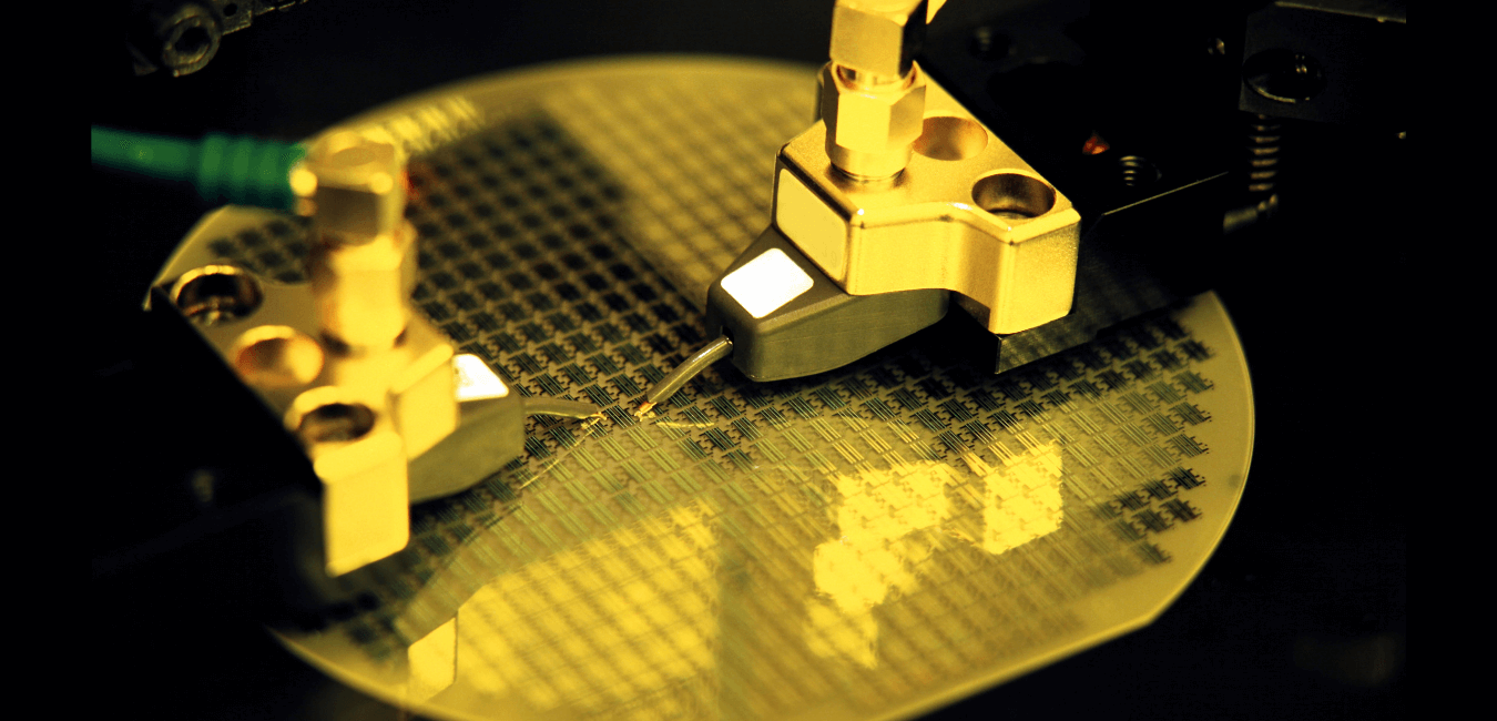
Once the logic and layout design has been created and testing completed, the circuit must be verified in a test run. This means that the circuit, which until now has only existed in the form of plans, is “cast” into the semiconductor material. For this purpose, the masks for exposure must be created with which the structures are transferred to the silicon, which is mainly used today, in the exposure systems. The silicon is available in so-called wafers, on which a large number of individual chips are produced. The individual circuits (dies) are usually tested on the wafer before this silicon wafer is cut into the individual dies.
During the first production tests, it is checked whether the planned circuit can be produced in this form at all and where any problems arise. Once the function test has been passed or the circuit has been revised accordingly, the individual dies must be wired and packaged. Since today’s microprocessors sometimes have over a thousand connections (pins) and one has to deal with the smallest structures, this undertaking is also not trivial. The task is to design the wiring in such a way that it functions without errors, but also that packaging can be carried out reliably, quickly and in a space-saving manner.
Once the individual practical tests have been passed and all steps have been optimized, series production can be tackled.
➡️ You can find more information on chip production, for example, at ASLM.
Chemical and physical backgrounds can be found at halbleiter.org.
At the end of August the 33rd Hot Chips Conference took place. Primarily exponents from the high performance chip scene meet and present the latest products and developments. If you are interested in the subject, you can find transcripts for (almost) all tracks at Anandtech:
➡️ https://www.anandtech.com/tag/hot-chips-33
In addition to many further developments of the large chip manufacturers, such as Intel, AMD and Nvidia, there are also innovations that will strongly influence the next chip generations. For example, new packaging techniques with increasingly granular 3D stacking or cache virtualization, as in IBM’s future mainframe processor Telum, which does without physical L3 and L4 caches.